Regulation 2021 Anna University Code – PH3251 deals with the semester – II Materials Science Syllabus of B.E Mechanical Engineering. Most of the semester syllabus tries to give both practical and theoretical knowledge to the students. To acquire the proper knowledge regarding the studies to prepare for the examination, need a detailed syllabus right?
This article will assist you in gaining most of the syllabus details. We tried our best to provide the required syllabus info. Chapter-wise syllabus along with reference books written by experts and textbooks added. Hence in this article Code – PH3251 Materials Science syllabus, we include all the details regarding the examination. Students can easily get all the data regarding the syllabus on one page. Hope you will understand the syllabus. And All the best for your exams. Don’t forget to share it with your friends.
If you want to know more about the syllabus of B.E Mechanical Engineering connected to an affiliated institution’s four-year undergraduate degree program. We provide you with a detailed Year-wise, semester-wise, and Subject-wise syllabus in the following link B.E Mechanical Engineering Syllabus Anna University Regulation 2021.
Aim Of Objectives:
- To make the students to understand the basics of crystallography and its importance in studying materials properties.
- To understand the electrical properties of materials including free electron theory, applications of quantum mechanics and magnetic materials.
- To instil knowledge on physics of semiconductors, determination of charge carriers and device applications
- To establish a sound grasp of knowledge on different optical properties of materials, optical displays and applications
- To inculcate an idea of significance of nano structures, quantum confinement and ensuing nano device applications.
PH3251 – Materials Science Syllabus
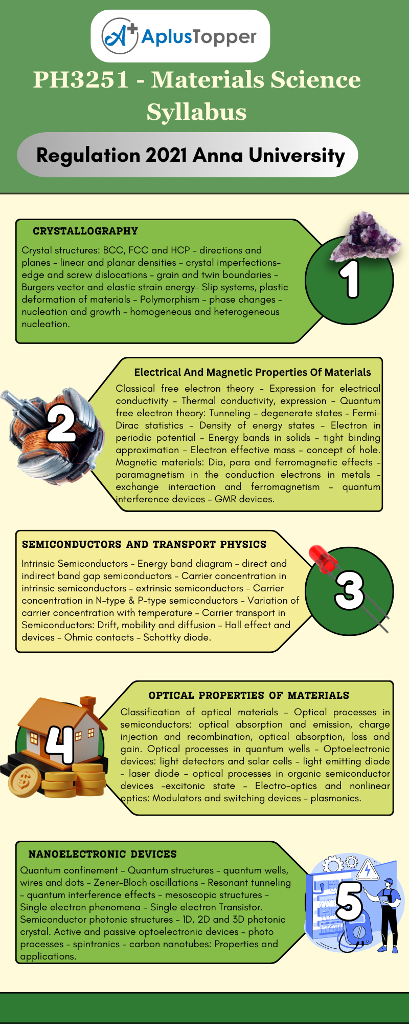
Unit I: Crystallography
Crystal structures: BCC, FCC and HCP – directions and planes – linear and planar densities – crystal imperfections- edge and screw dislocations – grain and twin boundaries – Burgers vector and elastic strain energy- Slip systems, plastic deformation of materials – Polymorphism – phase changes – nucleation and growth – homogeneous and heterogeneous nucleation.
Unit II: Electrical And Magnetic Properties Of Materials
Classical free electron theory – Expression for electrical conductivity – Thermal conductivity, expression – Quantum free electron theory: Tunneling – degenerate states – Fermi- Dirac statistics – Density of energy states – Electron in periodic potential – Energy bands in solids – tight binding approximation – Electron effective mass – concept of hole. Magnetic materials: Dia, para and ferromagnetic effects – paramagnetism in the conduction electrons in metals – exchange interaction and ferromagnetism – quantum interference devices – GMR devices.

Unit III: Semiconductors And Transport Physics
Intrinsic Semiconductors – Energy band diagram – direct and indirect band gap semiconductors – Carrier concentration in intrinsic semiconductors – extrinsic semiconductors – Carrier concentration in N-type & P-type semiconductors – Variation of carrier concentration with temperature – Carrier transport in Semiconductors: Drift, mobility and diffusion – Hall effect and devices – Ohmic contacts – Schottky diode.
Unit IV: Optical Properties Of Materials
Classification of optical materials – Optical processes in semiconductors: optical absorption and emission, charge injection and recombination, optical absorption, loss and gain. Optical processes in quantum wells – Optoelectronic devices: light detectors and solar cells – light emitting diode – laser diode – optical processes in organic semiconductor devices –excitonic state – Electro-optics and nonlinear optics: Modulators and switching devices – plasmonics.
Unit V: Nanoelectronic Devices
Quantum confinement – Quantum structures – quantum wells, wires and dots – Zener-Bloch oscillations – Resonant tunneling – quantum interference effects – mesoscopic structures – Single electron phenomena – Single electron Transistor. Semiconductor photonic structures – 1D, 2D and 3D photonic crystal. Active and passive optoelectronic devices – photo processes – spintronics – carbon nanotubes: Properties and applications.
Text Books:
- V.Raghavan. Materials Science and Engineering: A First Course, Prentice Hall India Learning Private Limited, 2015.
- S.O. Kasap, Principles of Electronic Materials and Devices, McGraw Hill, 2018.
- Jasprit Singh, Semiconductor Devices: Basic Principles, Wiley (India), 2007.
- Jasprit Singh, Semiconductor Optoelectronics: Physics and Technology, Mc-Graw Hill India (2019)
- G.W.Hanson. Fundamentals of Nanoelectronics. Pearson Education (Indian Edition), 2009.
References:
- R. Balasubramaniam, Callister’s Materials Science and Engineering. Wiley (Indian Edition), 2014.
- Wendelin Wright and Donald Askeland, Essentials of Materials Science and Engineering, CL Engineering, 2013.
- Robert F.Pierret, Semiconductor Device Fundamentals, Pearson, 2006
- Pallab Bhattacharya, Semiconductor Optoelectronic Devices, Pearson, 2017
- Ben Rogers, Jesse Adams and Sumita Pennathur, Nanotechnology: Understanding Small Systems, CRC Press, 2017.
Related Posts On semester – II:
- HS3252 – Professional English – II
- MA3251 – Statistics and Numerical Methods
- BE3251 – Basic Electrical and Electronics Engineering
